Amp Hours of Aural Entertainment

Just this week I was in a conversation with someone and I found myself saying “Hey The Amp Hour interviewed someone in that field!” only kill the flow of the conversation with Google searching for the episode. Turns out it was Episode 71 with John Edmond of Cree.

I started listening to The Amp Hour way back when the number of episodes could be counted your fingers in decimal, not binary. Since then I remember the gist of a lot of shows but I haven’t gone back and replayed too many which is a shame since Chris and Dave have done a lot of really cool interviews as the show has grown. After that conversation I figured if I can go back and reread books at any point why not do the same with podcasts? So that’s my aim for the short-term, re-listen to some of the interviews that have stuck with me over the years. It will shock no one that a lot, but not all, of them are analog focused.

#54 – An Interview with Jack Ganssle – Embedded Elchee Epexegesis

#60 – An Interview with Joe Grand – Pancyclopaedic Prototyping Polymath

#71 – An Interview with John Edmond – Luciferous LED Lucubrator

#77 – An Interview with Dr. Howard Johnson – Winsome Waveform Wizardry

#84 – An Interview with Bunnie Huang – Bunnie’s Bibelot Bonification

#95 – An Interview with Øyvind Janbu – Feracious Fabless Facilitator

#115 – An Interview with Dr Greg Charvat – Watcher of Wraithlike Walls

#117 – Interview with Alan Wolke – Undulating Utensil Utility

#119 – An Interview with Dr. Kent Lundberg – Luculent Linear Legacy

#129 – An Interview with Brett Fox and Dr Jeroen Fonderie – Device Doubling Decretum

#133 – An Interview with Ron Quan – Tenacious Transistor Teacher

#135 – An Interview with Mike Harrison – X-ray Examining Xenogogue

#144 – An Interview with Bob Davidson – Hoodied HP Hijinks

#157 – An Interview with the SparkFun Team – Efficacious Engineering Ensemble

#165 – An Interview with Henry Ott – Forced FCC Filtering

#171 – An Interview with Forrest Mims – Snell Solisequious Scientist

#180 – An Interview with Dave Taylor – Multi-talented Meter Maker

#181 – An Interview with Dave Vandenbout – Xceptional XESS Xenagogue

#187 – An Interview with Elecia White – Wirewove Worshipping Wookieist?

#196 – An Interview with Mike Engelhardt – SPICE Simulator Synteresis

Assuming I’m doing routine tasks at work that don’t require me to be in full on troubleshooting mode I should be able to keep occupied for a few weeks at least. If anyone can think of a good interview I forgot or just wants to share their favorite interview with me I’ll be happy to add it to the list! Also, I’d like to somehow bundle all these files into one convenient download for whoever wants them but I don’t know how to go about doing that easily unfortunately. Please clue me in if you could be so kind.

Update: Dave pointed out to me that I could always just use The Amp Hour App to easily find the shows I’m looking for. Doh! I’d forgotten all about that. Check it out and support the show!


Circuit Notes – Part 2

For my second Circuit Notes entry I decided to go with the Wien Bridge Oscillator. This time around the math wasn’t as intensive as it was for the Type III compensation with one exception. I had originally got the right answer in my derivation but had made a math error in the final step that I caught while writing in my Field Notes book. When I corrected the mistake I no longer knew how to make the math work out to give the correct output voltage at the resonant frequency. Wikipedia helped some by claiming RC was normalized to 1 but didn’t state why and I still don’t know. Is it just to make the math easier or is there a deeper reason for doing so?

Maybe college me could figure it out but present me is a tad rusty and so that last step is left as an exercise to the readers. I’ll keep digging and post an update if I find it or someone can correct me. Either way, the Evernote link can be found here and if you have any recommendations for a circuit you’d like to see analyzed feel free to send them my way.

Wien Bridge Oscillator

References:

http://en.wikipedia.org/wiki/Wien_bridge_oscillator

The Wien Bridge Oscillator


Circuit Notes – Part 1

The other week I impulse bought a bunch of Field Notes notebooks under the justification that they were a birthday gift to myself. I’ve been carrying a small pocket notebook on me for at least a year now so the regulator sized Field Notes won’t be stuffed in a drawer somewhere and forgotten but I also broke down and ordered a pack of the new limited release Arts & Sciences books too and needed a good use for them. They’re beautiful notebooks and I definitely recommend picking up a pack or two while you still can.

After brainstorming a bit I got the idea of using them to compose a circuit reference for myself. I seem to find my self deriving the same formulas over and over again at work so putting them all in one place where I can easily look back on them made the most sense. In order to keep this site from stagnating I figured I may as well also share them with whoever wants them. The Arts and Sciences books are the perfect size (7.5″ x 4.5″) and layout to fit a schematic on the blank left page and the derivation with some notes on the grid/lined right page. As an added bonus, writing out the circuits by hand with the idea of needing the info later will, ideally, help me to improve my normally atrocious penmanship as I have to take my time and focus on my writing.

Without further ado, here’s the Table of Contents and first entry into what I’m calling my Circuit Notes Series. I went with the transfer function for Type III compensation for switching regulators. Checkout the cool reference tables Field Notes threw on the inside cover too. Since this is just a reference I didn’t include all the math or in-depth details of how the circuit works, just some key notes to keep in mind. Think of this as an introduction to the circuit, not a be all end all treatise.

 Image

Image

For anyone who would like to save a digital copy of these derivations I’ve also posted these pages to Evernote (here and here) where you can add them to your own notebooks and search them using OCR. Hopefully someone finds these notes as useful as I do! The next note I do will be on an RC oscillator circuit and after that who knows? Recommendations for circuits are welcome too as I’m always willing to learn some new topology.

References:

Click to access tb417.pdf

Click to access slva633.pdf


If You Help an FAE…

In response to MarkAtMicrochip’s post about going down the rabbit hole that is helping FAEs. My story comes from the other side of the spectrum, a factory apps guy helping a field apps engineer. It’s definitely one-sided, biased, and not at all constructive but without further ado…

If you help an FAE

He’ll want you to provide a slew of measurements

If you send him off a the data

He’ll want to test the specs himself

If he goes off and tests the specs

When he’s finished

He’ll ask you some questions

That of course need answers yesterday because else the part won’t sell

When he gets your answers

He’ll notice the part suddenly doesn’t seem so competitive anymore

So he’ll probably ask you to bend the spec.

When he’s finished asking you to change the spec (again), he’ll need more input from marketing

He’ll start emailing

He might get carried away and promise things like pulling in schedules and higher sales

He might even demand a silicon spin

When he’s done, he might even want to change the specs again!

You’ll have to CYA in the email thread with talk of ways this will actually blow out the schedule and any potential issues that could arise

He’ll dig in, and demand some measurements you’ve already given him (twice)

He’ll probably tell you a story of being designed out

So you’ll spend days in the lab sweating and swearing and redesigning the circuit so it’s on the bleeding edge

When he sees the circuit he’ll get so excited he’ll want to show it to the customer. He’ll ask if you can reduce the BOM costs again though while still improving margin.

He’ll travel to the customer and test alongside them

In a lab

Then they’ll have trouble reproducing your results

Which means they’ll need

A detailed How To

He’ll take the detailed How To and throw it in recycling

When the board doesn’t quite work just right

He’ll have to try to troubleshoot it

He’s failed at this in the past!

So…

He does his “best” to make it work but it’s not his specialty

And chances are he can’t find time to finish the job

So he’s going to want you to help him.


Office Tomfoolery

So Monday at work I successfully pulled a prank on the designer for the part that is currently occupying the majority of my time. Concept, planning, and execution took about two weeks or so as I had to fit this little side project in around my real work obviously. Ever since the part’s inception this designer had been claiming it was perfectly designed and any errors were clearly the fault of me, the Applications Engineer. He wasn’t being mean or anything, this sort of good-natured rivalry is pretty common between the Apps and Design departments at work, but being that this is my first part as lead apps since starting a year ago meant I got some extra abuse. I figured it would be a good idea to go on the offensive and show everyone I wasn’t such an easy target. My boss, who’s been good friends with the designer for a long time now, thought it would be pretty funny and approved the gag, eager to see how it would play out.

The part is a single phase buck regulator meant for Vcore applications in laptops and ultrabooks. Vcore means that the regulator provides the main voltage rail to the processor, specifically an Intel one in this case as AMD and other processors have different power requirements. My goal was to somehow screw with the regulator, cause the output voltage to glitch and go out of spec, and convince the designer this was a silicon bug and not a board issue. After a little brain storming I came up with the following circuit which could be cobbled together out of various parts in the lab:
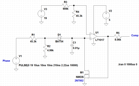
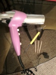
Prank Circuit

My Prank Circuit

Without diving down the rabbit hole that is regulator compensation, the comp pin of any buck converter is the output of an error amplifier which connects to a networks of passives going back to its negative terminal (the Feedback pin) and is part of the control loop used to keep the output voltage stable and well-regulated. My circuit would periodically drive this pin away from its steady state operating point. This disturbance would propagate through the chip and result in a noticeable glitch on the output voltage until the compensation loop could regain control and bring the output voltage back into spec.

As phase switches merrily along at the frequency and duty cycle set by the controller it gets divided down by R1 and R2. When phase is high the output of this voltage divider is enough to forward bias the diode and cause current to flow into C1 for a brief period before going low again. C1, which also connects to the positive input comparator U1, charges over time and when the voltage across the cap gets to be higher than the reference voltage present on the comparator’s negative input the comparator’s output swings to 5V. When U1’s output goes high two things happen. One, comp is driven away from steady state through R5 and two, the gate of M1 goes high which discharges C1 below the reference voltage starting the cycle over again.

Prank Sims

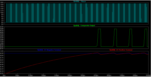
Prank Circuit Sim Results (Click to view properly)

There really wasn’t much thought process behind the component values in my circuit; they were determined through trial and error in simulation. I didn’t care how often the circuit would trigger, only that it did and the disturbances it caused would appear on Vout. One of my only goals was to ensure that the resistor dividers wouldn’t draw enough current to interfere with the normal operation of the regulator and cause it not to start up. My second goal was to “break” the regulator just enough to cause concern but not enough to trigger any of various over voltage, current, or temperature protections built into the chip. This is why R5 had to be added; without it comp was driven too hard and the part simply shutdown (there’s no fun in that).

With the circuit idea solidified I headed into the lab to jury rig it into place underneath one of the eval boards. It was a messy hour after work one day, but I successfully placed each component and wired in the various signals and voltages from all across the board. Once things got going, there would be so many cables and probes attached to the board I knew it wouldn’t get turned over until I was ready to reveal what I’d done.


Holding my breath I powered up the board after making all the necessary modifications. Surprisingly enough it worked! I hadn’t made any disastrous mistakes when wiring it all up and the resulting waveforms basically match with my sims. All that was needed was some tweaking of R5 to find the right value and I was ready for action.

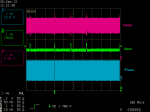
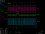
Cutting to Monday morning, I spent a little time taking scope captures of a good board and my doctored eval board. These were placed in a quick report which I shot off to my boss and the designer right after lunch. To add to the joke I took my clean scope caps using a part from an old rev of silicon and explained how the “bug” was only seen in the latest version of the chip. This caused the initial spark of concern in the designer as we’re currently waiting on a new rev of the chip to arrive from the fab and it was too late to make any changes. After getting some tests to run and tweaks to try, I actually went into the lab and did them! For one I was curious to see if any of them could actually fix the error (they didn’t) and secondly, this designer is pretty hands on and likes to come out to Apps Lab quite often. I knew that if he came out to see the glitch on the bench and none of his changes were made he would get suspicious. Fortunately, or unfortunately, other obligations kept him away for the day and he never came out to see the problem until the end of the day.

After running the initial list of tests the designer gave me I had a flash of brilliance that really threw him for a loop. I took a series of scope shots at each of the four switching frequencies our part could run at and varied the value of R5 at each one. Now I had created a problem that went away as switching frequency increased and could explain why we hadn’t seen this issue before as the majority of our testing had taken place at high frequency up until this point! Bingo.

By the end of the day, the designer was pretty much stumped. He’d done an initial check of his schematics, couldn’t spot an obviously fault he made, but thought it was a mistake somewhere in the core of the modulator. He told me that at this point he essentially resigned himself to hoping the new version of the chip came out okay and whatever changes he made would happen to fix this (remember it’s too late to make changes now as the part’s being fabricated).

Right afterwards I called him into the lab saying I’d found something interesting and he should come take a look. When I showed him the circuit on back of the board he didn’t get it at first. He asked why all this crap was added and what did it fix? I couldn’t hold back anymore and broke out in a smile and said that I just wanted to mess with him. Slowly realization dawned on him and he started laughing as did my boss and a few other guys in the lab who were in on the joke.

In the end the designer took it really well and thought it was pretty funny. He told my boss to give me more work as clearly I didn’t have enough to do since I could pull these elaborate pranks but mostly he just laughed. I now owe him a round or two the next time a bunch of us go out after work but that’s a price I’m more than willing to pay all things considered. In the end I caused him just enough trouble so he started to sweat but not enough to take him away from any real tasks he had to get done. A well executed prank overall in my opinion. Surely, there’s no way this will every come back to haunt me right?


iPad Repair – Quick, Dirty, Improvised

Fade In…

It’s the night of April 25, 2012. I sit in the big easy chair located in one corner of my living room browsing RSS feeds on my iPad and beginning to nod off. Deciding to turn in for the night I get up, switch off the lights, and set my iPad on the kitchen counter before going to lock the front door. No sooner am I two steps from the counter when I hear a thud as my iPad hits the ground.  Lame. I think aloud as I bend over and pick it up. Still bathed in darkness with sleep nibbling at the edge of my consciousness, I power it up and try out a few gestures to make sure everything still works. Everything checks out and I head to bed.

Fade to Black. Cut to this morning…

While waiting to take my girlfriend to the airport before work I open up my iPad with the intent of checking out a few odds and ends on the internet before we leave. Weirdly, the volume notification seemed to be stuck on the screen and nothing I could think off would get it off. Seeing the volume level stuck at the lowest it’s then I notice the dent on the top right corner, right where the volume rocker is. It seems in the fall last night the iPad caught it’s edge on one of the stools next to the counter somehow. As this realization dawned on me I let loose a string of expletives that could peel the paint off of walls and wonder if there’s anyway to fix this without dropping some serious coin. Without time to pursue the matter I head off to work…

 Fade to black…

Hope you enjoyed the melodramatic intro. I find it’s best to picture it in your mind like a film noir while reading it. Anyways, I made an appointment at the closest Apple Store to me when I got into work hoping the fact that the iPad (second gen by the way) was still under warranty would count for something. The dent wasn’t that bad from an aesthetics standpoint and if it occurred literally anywhere else on the device I wouldn’t have cared less. However, the iPad happened to fall and dent itself on one of the few areas that could actually affect functionality making it so I couldn’t ignore the problem. Murphy’s kind of a douche if you ask me.

When I got to the Apple Store they said I was out of luck. The warrant doesn’t cover accidental damage and all they could do was replace it for $250, take it or leave it. After leaving the store and a quick check on my phone for replacement back panels showed iFixit didn’t carry them and one random website sold them for $150. No luck there. Looking at the dent though I couldn’t help but think it was fixable if I sat down and tried. I went back asked the Apple employee if they could possibly let my in back to try but he rejected me. I said I swore I wouldn’t sue if it broke I just needed a small screwdriver. Again I got rejected so I went home full of piss and vinegar to try to tackle the repairs myself.

Looking over one of iFixit’s iPad 2 guides I saw they recommend heating the front panel with a heat gun to soften the glue before removing it and using guitar picks to hold the front panel up as you make your way along the edge. Well I don’t own either of those thing so I had to improvise. Girlfriend’s hairdryer, close enough? Toothpicks, why not? For the actual prying I was going to be doing I used one of the soldering picks I got from RadioShack ages ago.

Turning on the blow dryer I heated the corner of the iPad with the dent for about a minute or so, all the while keeping the nozzle ~1 inch from the iPad. A minute was all I needed to heat the tablet enough to make prying at the edge somewhat easy without using excessive force. Obviously if you’re removing the whole panel it’ll make longer to heat everything. Slowly and very gently I worked my pick into the device and applied pressure on the dent to pop it out. Every now and again I would fiddle with the volume rocker to see if it released at all giving me control over the volume again. When my initial prodding didn’t work I started to feed toothpicks into the crack I was creating to hold it open. I didn’t really have a plan in mind, I was mostly just slowly working on the dent and hoping volume control returned. Finally after ten minutes or so of playing around with various numbers of toothpicks stuck in my device I hit pay dirt. Volume control returned! Slowly with the pick I worked my way down the gap I had opened up and removed the toothpicks one by one.

Apologies for my awesome camera phone photography. It’s all I have to work with. Click a thumbnail to enlarge a picture.

After taking all the toothpicks out and seeing that the fix still worked I looked over my handy work. You can definitely tell the iPad was dented but overall things look good. There’s still a slight gap between the front and back covers which I may seal with some super glue or epoxy later but I’m not sure yet (my apologies to any Apple fanatic whose heart just skipped a beat). The RadioShack soldering pick worked pretty well but it did leave some scratches in the back panel. I would definitely recommend investing in some tools designed to open cases without leaving marks to anyone trying this themselves. I’ll probably wind up ordering some myself once my next paycheck hits just to have on hand. Also the toothpicks worked okay to keep the gap in the panels open but a few of their tips broke off and one may now be inside my iPad. Use them in a bind but invest in some guitar picks or similar item in my opinion.

Was this the greatest fix ever under taken? No, but I did save $250 dollars on a replacement, more if I wanted to upgrade to the new iPad, and I feel pretty damn happy about that. I’m now settling down with a cold beer (see the gallery above) and watching Community. I’ll leave you with this clip of Jeremy Clarkson from Top Gear that totally describes my current mood (0:15 to 0:50 is the most relevant chunk).


How to Stand Out & Other Career Fair Tips

A few weeks ago I traveled back to my alma mater to recruit some students for co-op and full-time positions available at various locations throughout my company. For the first time I was going to experience what it was like to stand on the employer side of the booth at a Career Fair. Chris Gammell, the good guy that he is, gave me some tips on getting through the day in one piece which came in quite handy. Fast forward to today and I can tell you that working a Career Fair is exhausting. I had fun and definitely plan on doing it again but I would almost say it’s easier to be the one looking for a job.

Regardless of how I feel personally about working Career Fairs, standing in that Field House all day I did see a few pitfalls that students fell into. Bearing in mine I’m not even close to a recruitment expert, read on for my take on what you the student can do to improve your game, standout, and sell yourself better to employers while attending a Career Fair. In no particular order they are:

  • Check out these tips from Chris Gammell. Go ahead, I’ll wait…
    • His post gives a lot of good advice and I pretty much agree with what he has to say (except for #4 when it comes to candy, that’s fair game) . Following his tips will definitely take you a long way when it comes it impressing potential employers.
  • Format your resume so it’s easy to read.
    • I looked at a lot of resumes during the 5 hours I was the Career Fair, a lot. There were long ones, short ones, pretty ones, and ugly ones. Some with one font, two fonts, red fonts, blue fonts. Okay, maybe that last part was a little bit of an exaggeration but I liked the Dr. Suess rhythm I had going. You’re only talking to an employer for a few minutes at most and those couple of minutes should be a discussion between you two rather than awkward fumbling and pointing as you try to locate and point out some portion of your resume after it’s come up in conversation.
    • Try and keep it to one page with only the most relevant information about yourself on it. Instead of listing every single course you’ve taken in school focus on work experience, skills, and projects you’ve done.
  • Highlight your big accomplishments that make you unique.
    • This goes along with my above point about relevant info on your resume. If you’re an upper level EE an employer should be able to assume you’re familiar with basic circuit theory. Showcasing the EE101 Resistor Divider Lab that everyone in 3 departments has to take is not making you stand out.
    • Have you taken a difficult elective not many others do? Were you also passionate about the work you did in that class? Talk about that instead.
      • VLSI and IC design course tend to really make you jump out to semiconductor companies. I know from both working the Career Fair and from my own job hunting experience. A hard copy of your layout will make even the toughest recruiter take you more seriously.
    • Did you solve a particularly interesting problem on an old internship or co-op? Be sure to mention that if it doesn’t come up on its own.
    •  Work on projects or study topics on your own or as part of a club? Those are both worth their weight in gold when it comes to standing out as it shows you’re passionate about the work you do and are self motivated. There’s also the possibility that a strong interest in your field outside of your required course work can make up for a less than stellar GPA or lack of on the job experience.
  • Be honest about what you like.
    • Our table was cluttered with all sorts of circuit boards and demo projects. Some were eval boards showcasing parts in our catalog and others were customer boards that had parts from our company designed in. Telling me one minute you like to design and work with electronics is one thing. However, if the next minute you’re not so much as batting an eye when I dig out an old intern project that has you doing just that doesn’t bode well for you. If you’re not thrilled about working with hardware (or software, or embedded systems, or MEMs, or whatever) don’t lead the recruiter on. It just wastes everyone’s time and it’s easy to see through.
  • Introductions are important.
    • You may not be the most outgoing person in existence and that’s okay. What’s not however is looking at the ground and mumbling your name during an introduction. The venue is going to be noisy to begin with and if the recruiter can’t catch your name after the first or second try it’s going to be tough not to put your resume in the pass pile. It’s sad but it’s true. 
    • Speak up, speak clearly, make eye contact, and have a firm handshake. It’s  simple things like that which can make you stand out after a recruiter has been on their feet all day dealing with Low-Talkers.
  • Come across as someone who is fun to work with. 
    • There was a second year student looking for their first co-op who whipped out a plate of homemade cookies and offered  them to all of us at the booth after we were done talking to him. That’s good stuff. We laughed, thanked him for offering, and once he was gone bumped his resume up a few spots on our list. Do you have to do something that extreme? No, but giving the impression working with you isn’t going to be hell counts for a lot.
  • Do at least some research as to who is looking to hire someone with your skills.
    • I work for an analog IC company. If you didn’t know that going into the Fair it was printed on our gigantic sign and the table was cluttered with all manner of circuit boards. The Co-op Office website had the list of majors we were interested in and so did the packets of info each student got upon entering the Fair. Odds are good we aren’t going to have openings for astronomers if all our material screams EE’s Wanted (yes, I was actually asked that).
    • If a company catches your eye you didn’t know existed until right that moment it’s okay to approach them and ask for more information, that’s why they’re at the Career Fair. There is however, a right and a wrong way to go about doing it.
      • Student A: “Hey, I’m an EE. What positions are available?” Isn’t going to cut it when there are people out there who are actually interested whatever the company does.
      • Student B: “Hi, my name is … I don’t know much about your company but I see your booth is covered in circuit boards. I really like working with electronics and would like to learn more about possibly getting a job with you guys.” This is almost word for word how a student introduced themselves to me at the Fair  and it’s a great example of how to approach a previously unheard of company.
      • Needless to say Student B got much more of my time than Student A did.
  • Don’t let employers push you around.
    • This tip is just something I encountered back when I was a student and want to pass along. On two occasions I had recruiters telling me how I was going to change my whole co-op schedule around and what courses to take to work  for them, after we had already established they stretched the truth about having hardware positions available. In these cases I politely interrupted the recruiter, said I wasn’t interested, and asked for my resume back if they hadn’t written on it (yes, it’s okay to do that once in a while).
    • Just as you shouldn’t waste an employers time they should be wasting yours. It’s better to spend your time  with companies that might actually have something for you (see also point #1 from Chris’ post).

Well there you have it, my take on Career Fairs and how you can avoid some of the mistakes that I witnessed during my first recruiting assignment. As I go out to other colleges and spend more time evaluating potential full-time and co-op candidates I’ll come back and revise and add to the list.

 Got any other tips for student job hunters? Did I miss the mark on any of my points? Just have a humorous Career Fair story from either side of the booth? Sound off in the comments.


Surgeon – My Fallback Career

So I was knuckle deep in a crazy board rework today at work trying to fit a 1206 cap where it didn’t belong because it was left off the schematic and consequently the layout. About halfway through I realized that the rework I was performing required a pretty steady hand, like I imagined a surgeon would need. I chuckled to myself and tweeted that if being an EE didn’t work out I was going to become a surgeon as all the reworks I’ve done over the years count as practice.

Satisfied with my wittiness I pocketed my phone and continued on modifying the board. That would be the end of the story if my brain would ever let anything go. Instead I kept thinking about surgery the rest of the day and realized that actually, EEs are quite a bit like surgeons when you think about it.

  • Operating Room & Table = Lab & Bench
  • Scalpel = X-acto Knife
  •  Heart Rate Monitor, O2 Monitor, etc. = Oscilloscopes, Multi-meters, etc.
  • Cauterization Tool = Soldering Iron
  • Nurses = Techs
  • Tweezers, Hemostats, Cotton Swabs = Tweezers, Hemostats, Cotton Swaps
  • Isopropyl Alcohol, Antiseptics = Isopropyl Alcohol, Board Cleaners
  • Anesthesia = Flux (Just makes the whole process a lot smoother)
  • Microscopic Surgery = Soldering & Scrapping under a microscope
  • Defibrillator = ESD Gun
  • Too much caffeine makes operating harder = ditto
  • Sinus Rhythm = Steady State Response

So I guess all that’s separating me from becoming a surgeon is jargon am I right?


More Vintage Tek Gear

Back in October I posted about some old Tektronix equipment I found at work consisting of a function generator and current probe amps sitting in a power supply chassis. Well after a few more months of rummaging around the various labs and store rooms at work I stumbled across another old piece of Tektronix memorabilia, a Type 576 Curve Tracer. As far as I can tell from perusing the web it dates back to the late 1950’s or early 1960’s. One site, Barry Tech, claims the curve tracer is from 1969 while Vintage Tek simply states the 576 was developed sometime between 1960 and the early 70’s when the series was discontinued. The 576 is also the second curve tracer offered by Tekronix designed with transistors instead of tubes, the first being the 575.

[Update: The guys over at Vintage Tek got in touch with me and as it turns out the 576 first appeared in the March 1969 Tektronix catalog.]

Spec Overview from the datasheet found on Valuetronics:

  • Can deliver up to 220W of peak power to the DUT.
  • Voltage steps can be as large as 1500 V and current steps can hit 20A peak. If you purchase the 176 high current plug-in the 576 can hit up to 200A!
  • Absolute accuracy of 2% of total output including settling, or 1% of amplitude setting.
  • Pulse generator capable of 1 to 10 repeated steps.
  • Built in beta and gm calculator to save the designer from pesky arithmetic

The 576 Curve Tracer in all its magnificent glory. Couldn't find a picture of the insides online sadly.

I think I definitely prefer knobs over touchscreens on my test equipment. Fiddling with this guy just felt great. Not that I want to give up my modern gear completely mind you, I'm just sayin'.

Note the force and sense lines for the collector and emitter terminals. Also this thing could dish out some serious power to the DUT, up to 220W!

Looking on Barry Tech I saw they also provided a link to the 576’s manual you can check out here. Tek was kind enough to provide a complete section dedicated to the circuit description that I definitely plan to check out in my free time. The circuit description section includes pieces on the control loop compensation, logic diagrams, timing charts, and at first glance, what appears to be pretty detailed explanations of it all. Check out Figure 3-6 to see a diagram of the discrete A/D used in the tracer designed with only a handful of diodes and resistors. Supporting the DIY movement before it was fashionable, the manual also contains a complete section on basic maintenance and troubleshooting including where to locate various circuits, key performance specs, and a soldering guide.

Unfortunately I don’t think this 576 sees much action anymore at work. To my knowledge nothing in our product catalog needs to be tested using at the individual device level and if it did it would probably be done using a wafer probe station instead. I’ll ask some of the designers and test engineers if it’s ever used anymore and report back.


Jim Williams, AN13, & Op Amp Wizardry

Not too long ago I was reading through one of Jim Williams’ famous App Notes, AN13, High Speed Comparator Techniques. It’s an older App Note that was published back in 1985 and I didn’t really have a specific reason for reading it other than thinking it looked interesting and I wanted to learn more about comparators. For a comprehensive overview of AN13 I recommend reading Dr. Lundberg’s (aka Dr. Analog) three part summary over on his blog Reading Jim Williams.

The first section of AN13 is extremely informative and makes the app note well worth the read in my opinion. Entitled “The Rouges Gallery of High Speed Comparator Problems” this portion of the app note highlights common pitfalls of comparator circuits including bypassing, ground planes, probe compensation, and much more. As useful as The Rouges Gallery is what intrigues me the most in AN13 doesn’t actually have anything to do with comparators and is found in the first circuit of the Applications Section. The overall circuit is a Voltage to Frequency Converter shown in Figure 16 of AN13 and reproduced below with the part that fascinates me most boxed in red.

What Jim Williams has done is replace the input stage of A1, the LT318A, with a pair of 2N4393 JFETs. These JFETs drive the output stage of A1 via the two Comp pins of the amplifier. A1’s true inputs are shutdown by shorting them directly to the -15V supply leaving the rest of the amplifier free to serve Williams’ needs for this particular application. According to page 8 of the app note this trick was done “for low bias, high-speed operation.”  Now I don’t have a whole lot of experience using op amps with Comp pins to begin with let alone understand their internal architecture enough to hack them like Jim did. As far as I knew something like this wasn’t even possible and it definitely wasn’t brought up in any of the classes I took in school! Needless to say, upon seeing it done here in AN13 I was a little stunned.

After my initial shock I decided to look at the LT318A a little more closely to try to see how Jim Williams had pulled off this neat little trick. Linear Tech is usually pretty good about providing schematics  of their op amps with a description in their datasheets and I was hoping this was the case with the 318. As it turns out, the LT318A datasheet is a bit sparse compared to other datasheets from Linear but fortunately for me it does contain a schematic of the part. Unfortunately for me, it doesn’t appear to be a simplified version and there isn’t a functional description. Looking at the schematic in detail I could tell this wasn’t the basic op-amp architecture I was used to dealing with but I decided to dive in anyways. I’ve copied the LT318A schematic here and marked it up into functional blocks as best as I’m able to but if anyone out there has more info on this op amp or sees somewhere that I went wrong please let me know.

From studying the datasheet schematic of the LT318A I was able to understand more of how Jim’s op amp hack works. Connecting the amps inputs on pins 2 and 3 to the negative rail turns off the differential amplifier, the heart of which are the input transistors Q1-Q4 with Q13 and Q14 being the active loads. As a side note there may be some common-mode feedback on the diff pair but I’m not 100% sure. Thinking about what was said in the app note I would have to assume using two JFETs in place of the input circuit on the op amp would lower bias requirements and cutting out all those transistors speeds up operation of the overall application circuit.

The output from the input differential stage is then fed into what I assume to be a second gain stage  (not sure what Q21 does, this may be a weird folded cascode configuration too). From Figure 16 in AN13, you can see that Jim Williams has the JFET input transistors driving pins 1 and 5 on the LT318A. Sure enough these two pins correspond to the output of the diff pair on the amplifier and feed directly into the second gain stage. Following the gain stage comes what appears to be a Class AB output stage.

I enjoyed this little exercise of trying to understand some of Jim Williams’ techniques. While I may not have exactly figured out how the LT318A works I feel I did understand the high-level thought process behind this neat little trick. I also saw that my BJT design skills are a little rusty and that perhaps I should dust off Gray & Meyer or Sedra-Smith and brush up on the topic. Who knows, there could be a revisit to this post in the future…

Any neat op amp hacks of your own? See a mistake in my analysis of the LT318A? Let me know in the comments. Oh, and Happy New Year!